1. Fundamental Properties and Nanoscale Actions of Silicon at the Submicron Frontier
1.1 Quantum Confinement and Electronic Framework Makeover
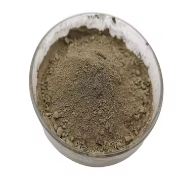
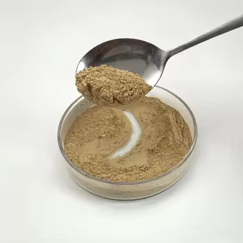
(Nano-Silicon Powder)
Nano-silicon powder, made up of silicon bits with characteristic dimensions below 100 nanometers, stands for a standard change from mass silicon in both physical actions and practical energy.
While bulk silicon is an indirect bandgap semiconductor with a bandgap of roughly 1.12 eV, nano-sizing induces quantum confinement effects that basically change its digital and optical homes.
When the particle size approaches or drops below the exciton Bohr span of silicon (~ 5 nm), fee providers become spatially constrained, causing a widening of the bandgap and the development of visible photoluminescence– a phenomenon missing in macroscopic silicon.
This size-dependent tunability makes it possible for nano-silicon to emit light across the visible range, making it an appealing prospect for silicon-based optoelectronics, where standard silicon stops working as a result of its inadequate radiative recombination effectiveness.
In addition, the increased surface-to-volume proportion at the nanoscale boosts surface-related phenomena, including chemical sensitivity, catalytic activity, and communication with electromagnetic fields.
These quantum effects are not merely scholastic inquisitiveness yet form the foundation for next-generation applications in energy, picking up, and biomedicine.
1.2 Morphological Variety and Surface Chemistry
Nano-silicon powder can be synthesized in different morphologies, consisting of round nanoparticles, nanowires, porous nanostructures, and crystalline quantum dots, each offering distinct advantages depending on the target application.
Crystalline nano-silicon usually maintains the ruby cubic structure of bulk silicon yet displays a higher density of surface area flaws and dangling bonds, which have to be passivated to stabilize the product.
Surface area functionalization– frequently achieved with oxidation, hydrosilylation, or ligand add-on– plays an essential role in identifying colloidal stability, dispersibility, and compatibility with matrices in compounds or organic settings.
For instance, hydrogen-terminated nano-silicon reveals high sensitivity and is prone to oxidation in air, whereas alkyl- or polyethylene glycol (PEG)-coated bits display enhanced stability and biocompatibility for biomedical usage.
( Nano-Silicon Powder)
The presence of a native oxide layer (SiOₓ) on the fragment surface area, also in minimal amounts, dramatically influences electric conductivity, lithium-ion diffusion kinetics, and interfacial reactions, especially in battery applications.
Understanding and regulating surface chemistry is therefore essential for taking advantage of the complete potential of nano-silicon in functional systems.
2. Synthesis Strategies and Scalable Fabrication Techniques
2.1 Top-Down Approaches: Milling, Etching, and Laser Ablation
The production of nano-silicon powder can be extensively categorized into top-down and bottom-up approaches, each with unique scalability, purity, and morphological control characteristics.
Top-down strategies involve the physical or chemical decrease of bulk silicon right into nanoscale fragments.
High-energy round milling is a widely utilized commercial method, where silicon pieces undergo intense mechanical grinding in inert atmospheres, leading to micron- to nano-sized powders.
While affordable and scalable, this approach frequently introduces crystal issues, contamination from crushing media, and wide fragment dimension circulations, needing post-processing filtration.
Magnesiothermic decrease of silica (SiO TWO) adhered to by acid leaching is one more scalable course, especially when making use of natural or waste-derived silica sources such as rice husks or diatoms, offering a sustainable path to nano-silicon.
Laser ablation and responsive plasma etching are a lot more precise top-down approaches, with the ability of producing high-purity nano-silicon with regulated crystallinity, however at greater price and lower throughput.
2.2 Bottom-Up Approaches: Gas-Phase and Solution-Phase Development
Bottom-up synthesis allows for greater control over particle dimension, shape, and crystallinity by constructing nanostructures atom by atom.
Chemical vapor deposition (CVD) and plasma-enhanced CVD (PECVD) allow the growth of nano-silicon from gaseous forerunners such as silane (SiH ₄) or disilane (Si ₂ H ₆), with criteria like temperature, stress, and gas circulation dictating nucleation and growth kinetics.
These approaches are particularly effective for creating silicon nanocrystals embedded in dielectric matrices for optoelectronic devices.
Solution-phase synthesis, including colloidal courses using organosilicon compounds, allows for the manufacturing of monodisperse silicon quantum dots with tunable exhaust wavelengths.
Thermal disintegration of silane in high-boiling solvents or supercritical liquid synthesis likewise generates top notch nano-silicon with narrow dimension circulations, ideal for biomedical labeling and imaging.
While bottom-up approaches generally generate superior worldly quality, they deal with challenges in large production and cost-efficiency, demanding recurring research into hybrid and continuous-flow procedures.
3. Power Applications: Changing Lithium-Ion and Beyond-Lithium Batteries
3.1 Function in High-Capacity Anodes for Lithium-Ion Batteries
Among one of the most transformative applications of nano-silicon powder hinges on energy storage, particularly as an anode product in lithium-ion batteries (LIBs).
Silicon uses a theoretical specific capacity of ~ 3579 mAh/g based upon the formation of Li ₁₅ Si ₄, which is almost ten times more than that of conventional graphite (372 mAh/g).
Nevertheless, the large quantity expansion (~ 300%) during lithiation triggers bit pulverization, loss of electrical call, and constant solid electrolyte interphase (SEI) development, causing fast capacity fade.
Nanostructuring alleviates these problems by shortening lithium diffusion paths, fitting strain better, and decreasing crack chance.
Nano-silicon in the kind of nanoparticles, permeable frameworks, or yolk-shell structures makes it possible for relatively easy to fix biking with enhanced Coulombic performance and cycle life.
Commercial battery modern technologies currently integrate nano-silicon blends (e.g., silicon-carbon compounds) in anodes to improve energy thickness in consumer electronics, electrical vehicles, and grid storage space systems.
3.2 Prospective in Sodium-Ion, Potassium-Ion, and Solid-State Batteries
Beyond lithium-ion systems, nano-silicon is being checked out in arising battery chemistries.
While silicon is much less responsive with sodium than lithium, nano-sizing enhances kinetics and enables minimal Na ⁺ insertion, making it a prospect for sodium-ion battery anodes, especially when alloyed or composited with tin or antimony.
In solid-state batteries, where mechanical security at electrode-electrolyte interfaces is important, nano-silicon’s ability to undertake plastic contortion at little ranges reduces interfacial stress and anxiety and enhances contact maintenance.
In addition, its compatibility with sulfide- and oxide-based strong electrolytes opens avenues for safer, higher-energy-density storage space remedies.
Research remains to optimize interface design and prelithiation approaches to make best use of the long life and effectiveness of nano-silicon-based electrodes.
4. Emerging Frontiers in Photonics, Biomedicine, and Composite Products
4.1 Applications in Optoelectronics and Quantum Source Of Light
The photoluminescent residential properties of nano-silicon have revitalized efforts to develop silicon-based light-emitting devices, an enduring difficulty in incorporated photonics.
Unlike bulk silicon, nano-silicon quantum dots can show effective, tunable photoluminescence in the noticeable to near-infrared range, making it possible for on-chip lights compatible with corresponding metal-oxide-semiconductor (CMOS) modern technology.
These nanomaterials are being integrated right into light-emitting diodes (LEDs), photodetectors, and waveguide-coupled emitters for optical interconnects and sensing applications.
Furthermore, surface-engineered nano-silicon exhibits single-photon discharge under particular problem setups, positioning it as a potential platform for quantum information processing and protected communication.
4.2 Biomedical and Environmental Applications
In biomedicine, nano-silicon powder is gaining attention as a biocompatible, naturally degradable, and safe alternative to heavy-metal-based quantum dots for bioimaging and medication distribution.
Surface-functionalized nano-silicon bits can be designed to target particular cells, release healing representatives in feedback to pH or enzymes, and supply real-time fluorescence tracking.
Their deterioration into silicic acid (Si(OH)₄), a naturally happening and excretable compound, lessens long-lasting poisoning issues.
Furthermore, nano-silicon is being explored for ecological remediation, such as photocatalytic destruction of toxins under visible light or as a decreasing agent in water treatment procedures.
In composite products, nano-silicon boosts mechanical strength, thermal security, and wear resistance when included right into steels, ceramics, or polymers, especially in aerospace and auto elements.
To conclude, nano-silicon powder stands at the intersection of basic nanoscience and commercial innovation.
Its unique combination of quantum impacts, high reactivity, and flexibility across power, electronic devices, and life sciences emphasizes its function as an essential enabler of next-generation technologies.
As synthesis techniques development and assimilation difficulties are overcome, nano-silicon will certainly continue to drive progress toward higher-performance, lasting, and multifunctional material systems.
5. Distributor
TRUNNANO is a supplier of Spherical Tungsten Powder with over 12 years of experience in nano-building energy conservation and nanotechnology development. It accepts payment via Credit Card, T/T, West Union and Paypal. Trunnano will ship the goods to customers overseas through FedEx, DHL, by air, or by sea. If you want to know more about Spherical Tungsten Powder, please feel free to contact us and send an inquiry(sales5@nanotrun.com).
Tags: Nano-Silicon Powder, Silicon Powder, Silicon
All articles and pictures are from the Internet. If there are any copyright issues, please contact us in time to delete.
Inquiry us
